
Non-Destructive Screening Before SEM or TEM
How optical screening can help you choose where to look—and make each detailed inspection more useful.
A high-resolution image can tell you a great deal about one location on a wafer. The harder question is whether that location represents the material you are trying to understand.
For teams developing diamond substrates, semiconductor materials or thin films, choosing where to inspect is part of the measurement problem. A defect might sit near an edge, follow a polishing track or cluster in one region. Examining a few convenient locations can leave that larger pattern unexplored.
Non-destructive optical wafer screening offers a practical starting point: map a defined area, identify candidate anomalies and carry their coordinates into more detailed analysis. This gives scanning electron microscopy (SEM) and transmission electron microscopy (TEM) a better-informed set of questions to answer.
Build a map before choosing a close-up
Optical inspection and electron-beam review already work together in semiconductor manufacturing. KLA, for example, combines optical inspectors with an electron-beam review system for defect discovery and classification. The value of this division of work is broad coverage followed by targeted investigation. KLA: Defect Discovery
Depending on the instrument and material, optical measurements can reveal particles, scratches, pits, surface variation and changes in reflectance or phase. Those signals help identify where a surface differs from its surroundings. They do not automatically establish the physical cause of every anomaly. KLA: Wafer Defect Inspection and Review
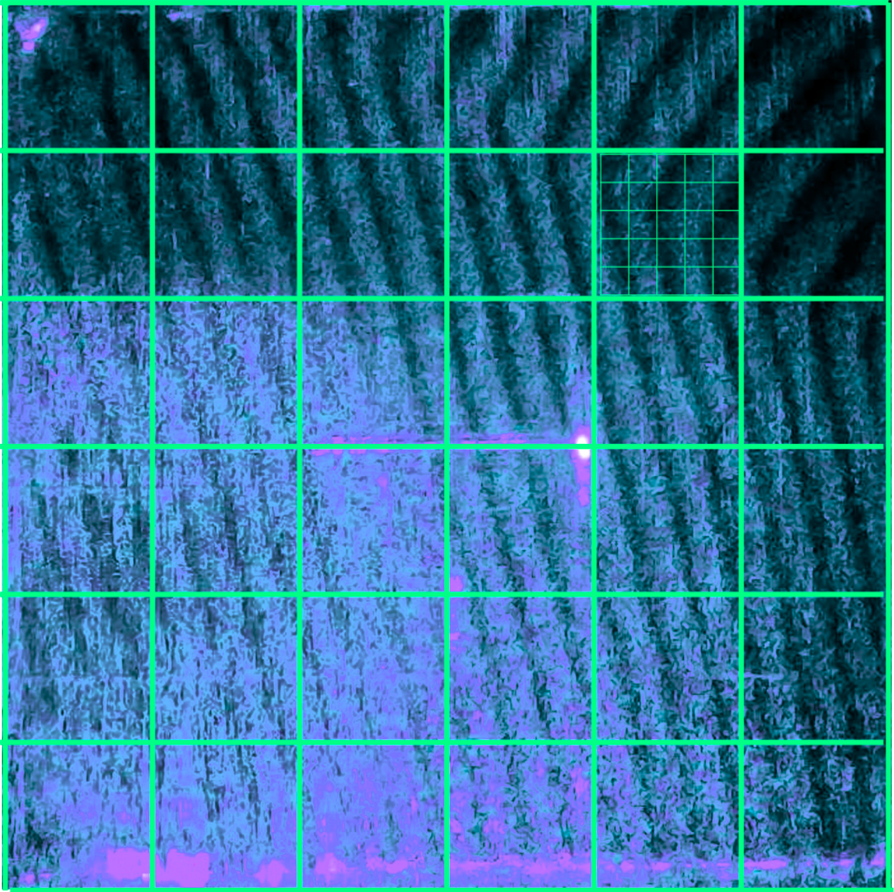
Consider a diamond wafer being evaluated after polishing. A useful initial screen would map candidate surface features, show whether they cluster and preserve their locations for follow-up. The team could then examine selected features alongside ordinary-looking regions to learn which optical signatures correspond to meaningful defects.
The important output is a traceable map: what was examined, what was flagged and where the next instrument should look.
Preserve the sample and choose preparation deliberately
SEM does not always require conductive coating or destructive preparation. Suitable operating conditions can allow uncoated samples to be examined, including some nonconductive materials. Charging, vacuum compatibility and the required analysis determine the preparation needed. Thermo Fisher describes conductive coating and reduced-vacuum operation among the available options. Thermo Fisher: SEM Sample Preparation
Preparing a cross-sectional TEM specimen from a bulk wafer is a different commitment. Focused ion beam milling can extract and thin material from a selected region, altering that location. Choosing the region carefully matters before preparation begins. JEOL: FIB TEM Specimen Preparation
An optical baseline recorded beforehand preserves information about the surface in its earlier condition. It can also support comparisons before and after a process step, provided the same locations and measurement conditions can be reproduced.
Make screening accountable to the next measurement
A practical pilot should answer four questions:
What must the screen detect? Define the defect classes, relevant sizes and consequences of missing them. A method suitable for polishing damage may be unsuitable for buried interfaces.
Where did you actually look? Record inspected area, uninspected regions, acquisition settings and coordinates. Check that another instrument can relocate the flagged features.
What did the screen miss? Validate flagged sites and a planned selection of unflagged sites. Checking only the most striking images can hide false negatives.
Did the combined workflow improve? Compare total preparation, imaging, relocation and analysis time while tracking missed defects and unnecessary follow-up.
A clean optical map means that no qualifying signal was detected under the stated conditions. It cannot, by itself, certify that a wafer is defect-free. Optical screening also should not become a gate that excludes electron microscopy when the defect of interest produces no reliable optical signature.
Where NanoFraction fits
NanoFraction is developing optical and computational methods for non-destructive materials characterization. Our diamond wafer work explores how optical signatures can locate candidate defects and describe surrounding surface structure.
For a customer pilot, the objective is to establish whether those measurements improve inspection decisions on that customer's material. We would compare optical findings with an agreed reference method, test repeatability and determine which signals justify further investigation.
The opportunity is to cover more relevant area, direct detailed microscopy toward better-selected locations and retain evidence that connects each close-up to the wider sample. Any reduction in cost or turnaround time must be demonstrated across the complete workflow, including the screening step itself.
If your team is deciding where to spend its next SEM session or which location deserves a TEM cross-section, NanoFraction can help evaluate an optical screening step using representative samples and existing reference measurements. Discuss your application.